Dual wavelength Y-junction glass integrated waveguides for mm-wavecarrier generation
Arab N1, Poette J1, Bastard L1, Broquin J-E11Univ. Grenoble Alpes, CNRS, Grenoble INP, IMEP-LAHC, 38000 Grenoble, Francee-mail: julien.poette@grenoble-inp.fr
ABSTRACT
This paper presents the use of co-integrated lasers on glass for the generation of radio-frequency carriers byoptical heterodyning. By using the ion exchange glass platform, two DFB lasers and a power combiner have beenfabricated on a single substrate. Thanks to the excellent thermal stability of these lasers, a drift of the beatingsignal frequency as low as 5 MHz has been measured without any thermal regulation. These performancesrepresent an improvement by several orders of magnitude when compared to heterodyned semiconductor laserstechnology and have the potential to generate mm-wave carrier frequencies up to a few THz.
Low Polarization Sensitive Semiconductor Optical Amplifier Co-Integrated with Passive Waveguides for Optical Datacom and Telecom Networks Student Paper
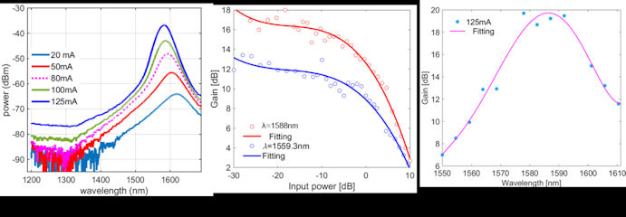
Aref Rasoulzadeh Zali1, Steven Kleijn2, Luc Augustin2, Ripalta Stabile1, Nicola Calabretta11IPI-ECO research institute, Eindhoven University of Technology, Eindhoven, theNetherlands2Smart Photonics, High Tech Campus, Eindhoven, theNetherlands E-mail: a.rasoulzadehzali@tue.nl
ABSTRACT
For device application in Datacom and Telecom networks, low polarization sensitive (PS) SOAs with easy fabrication process co-integrated with passive photonic circuits are highlyessential.In this work,alow polarization sensitive SOA based on a bulk active layer is designed, fabricated and characterized. Theresults of the present work focuson the investigation of low polarization ridge waveguideswith bulk active layer. In the proposed structure,the SOA is integrated with other passive waveguides, thereforeexhibitingits potential application to be integrated in a photonic integrated circuit. The low polarization sensitivity of bulk SOA is provenfora wide range of input power (-25dBm to 10 dBm) and wavelength for network-device applications. Characterizations of anSOA with length of 1.5mmco-integrated with 2.3 and 0.8mm passive waveguides indicate 17dB net gain with a polarization dependent gain (PDG) between 0.3dB and 3dB at 1588nm wavelength and 125mA bias currentfor different input optical powers.
Bifurcation and Chaotic Behavior of Feedback Semiconductor Lasers Operating in the Full Range of External Reflectivity
Qin Zou, Kamel Merghem,Badr-Eddine Benkelfat, Musharrat ShabnamSamovar, CNRS, Télécom SudParis, Institut Polytechnique de Paris,19 place Marguerite Perey, 91120 Palaiseau, Francee-mail:qin.zou@telecom-sudparis.eu
ABSTRACT
We investigatethe properties of a semiconductor laser with arbitrary levels of external optical feedback,by means of an iterative travelling-wave (ITW) model. Bifurcation diagrams andthe corresponding Lyapunov exponent areused to describethe behavior of the feedback laser as the external feedback reflectivity increases from 0 to 1. Similarities and differences between the ITW model and the Lang-Kobayashi (LK) modelare also reviewed. To determine the critical value of the external reflectivity, beyondwhich the LK model would no longer be valid, we propose a criterion based on the iterates of the phase mapsfor both the compound-cavity modes(ITWmodel) andthe external-cavity modes(LKmodel).Preliminary results show that this critical value may correspond to the so-called «-value»,which is defined as the onset value of the first chaotic region.
Download poster
Narrow-Linewidth DBR Laser Using Open-Access High-Precision Gratingin InP PIC Generic Foundry Platform
Julio Darío López1, Dan Zhao2,3, Mu-Chieh Lo4,∗, Robinson Guzmán1,,Xaveer Leijtens2, and Guillermo Carpintero11Universidad Carlos III de Madrid, Leganés, Spain2Technische Universiteit Eindhoven, Eindhoven, Netherlands3now with ASML, Veldhoven, Netherlands4University College London, London, UK*e-mail: m.lo@ucl.ac.uk
ABSTRACT
In this paper, we present DBR lasers using DUV lithography in a generic InP-based photonic integrationplatform. The DBR lasers exhibit SMSR over 45 dB and laser linewidths below 100 kHz
Design of hybrid lasers for silicon photonics: efficiency, optical feedback tolerance and laser dynamics
Mariangela Gioannini1, Lorenzo Columbo1, Antonino Bologna1, Marco Novarese1, Sebastian Romero-García2, Dominic Siriani2, Jock Bovington21 Department of Electronics and Telecommunication, Politecnico di Torino (Italy) 2Cisco Systems, San Jose, CA, (US) e-mail: mariangela.gioannini@polito.it
ABSTRACT
We present the design and the simulation of the dynamics of hybrid lasers based on a reflective SOA edge-coupled to a silicon photonics integrated reflector realized with waveguide rings. We design the laser for high efficiency and tolerance to spurious optical feedback and we compare the best designs in SiN and SOI platforms. By simulating the laser dynamics with a Time Domain Travelling Wave approach we show that the hybrid solitary laser (ie: without feedback) can operate in various regimes from CW to self-pulsing. These regimes are triggered by the linewidth enhancement factor of the SOA and can be controlled by a phase control section. The tolerance to the optical feedback is also further enhanced by the damping of the relaxation oscillations filtered by the narrowband reflector.
Design of III-V on Silicon OpticalSwitch based on Mach-ZehnderandSOA Switching Elements
Junfei Xia,Qixiang Cheng,Tongyun Li, Richard V. PentyCentre for Photonic Systems, Electrical Engineering Division, Department of Engineering, University of Cambridge, 9 JJ Thomson Avenue, Cambridge CB3 0FA, UK.e-mail: qc233@eng.cam.ac.uk
ABSTRACT
This paper proposes a novel lossless photonic switch based on III-V semiconductor optical amplifiers(SOAs) combined with silicon photonics in a heterogenerousintegrationscheme. An 8×8 device implemented usingdilated Banyan topology achieves a 17dB input power dynamic range(IPDR) withpower penaltiesof less than 1dB. Silicon-based thermo-optic(T-O)Mach-Zehnder (MZ) switching elements are used to manipulate light, whilstSOAs are placed in the middle to switch in tandem with the MZs to provide gain and crosstalk suppression. A 64×64 Clos switchbuilt from the 8×8 blocks exhibits a 10dB IPDR with power penalties of less than 1dB.
Manufacture-compliant InP-based metal cavity nanolaser designStudent Paper
E. Malysheva, A. Fiore, K.A. Williams, V.Dolores-CalzadillaInstitute for Photonic Integration, Eindhoven University of Technology, Eindhoven, The Netherlandse-mail: e.malysheva@tue.nl
ABSTRACT
Nanolaser cavity structures are very sensitive to fabrication non-idealities. One of the important aspects is the cavity sidewalls non-verticality, produced with reactive ion etching, which have an impact on total opticallosses. In this work the influence of etching slopes on the lasing performance is studied, and novel nanolaser cavity design on InP Membrane on Silicon platform with increased etching slopes tolerance is proposed. For cavity with width 800 nm and length 1000 nm threshold gain remains less than 1000 cm-1 for etching slopes up to 2 degrees.
Monolithically Integrated Wavelength Tunable Dual Comb Source usingGain Switching(Student Paper)
Jack Mulcahy1,2, John McCarthy1,2, Mohamad Dernaika3, Albert A. Ruth4, Satheesh Chandran4,Prince M. Anandarajah5, Eamonn P. Martin5, Justin K. Alexander6& Frank H. Peters1,21Tyndall National Institute, Lee Maltings, Cork, Ireland2Physics Department, University College Cork, Cork, Ireland3Rockley Photonics Ireland, Lee Mills House, Lee Maltings, Cork, Ireland4Physics Department & Environmental Research Institute, University College Cork, Cork, Ireland5School of Electronic Engineering, Dublin City University, Glasnevin, Dublin 9, Ireland6Aeponyx, Montreal, QC, Canadae-mail: jack.mulcahy@tyndall.ie
ABSTRACT
A monolithically integrated dual output optical comb source is demonstrated by gain switching two separateinjection locked Fabry P ́erot lasers. The device consists of the two slave lasers and a master laser separated bya multi-mode interference coupler. Wavelength tunability has been demonstrated by varying the electrical biasof the master laser, which consists of three electrically isolated sections. Combs were generated and recordedfor multiple wavelengths from each slave laser.
Perovskite Nanocrystals:an Active Material for Integrated Optics(Student Paper
Juan Navarro-Arenas, 1Andrés F. Gualdrón-Reyes,2-3Vladimir S. Chirvony, 1Iván Mora-Seró,2Juan Martínez-Pastor1and Isaac Suárez 41Instituto de Ciencia de Materiales (ICMUV), Universidad de Valencia, C/ Catedrático José Beltrán, 2, 46980 Paterna, Spain.2Institute of Advanced Materials (INAM), University Jaume I, Avenida de Vicent Sos Baynat, s/n, 12006 Castelló de la Plana, Castellón, Spain.3Biofuels Lab-IBEAR, Faculty of Basic Sciences, University of Pamplona, Pamplona, Colombia. C. P. 543050.4Escuela Técnica Superior de Ingeniería, Universidad de Valencia, C/Avenida de la Universidad s/n 46100 Burjassot, Valencia, Spain.e-mail: juan.navarro-arenas@uv.es
ABSTRACT
Perovskite nanocrystals(PNCs)have demonstratedextraordinary capabilities to construct a new generation of optical sources and amplifiers. In this paper, we firstly analyze the optical gain properties of these materials, and then report our advances towards their integration in integrated optics devices.
An Accurate Characterization Method for Polarization Converters on theIndium Phosphide Membrane on Silicon Platform(Student Paper)
Sander Reniers1, Kevin Williams1, Jos van der Tol1, Yuqing Jiao11Institute for Photonic Integration (IPI), Eindhoven University of Technologye-mail: s.f.g.reniers@tue.nl
ABSTRACT
In this paper, an accurate characterization method for characterization of the conversion efficiency of polar-ization converters on the InP-membrane-on-silicon (IMOS) platform is demonstrated. The method is insensitiveto propagation losses, device insertion loss and grating coupler insertion loss. Circuits for demonstration of themethod with polarization converters with various parameters are fabricated. A conversion efficiency as high as97.5±0.7% is experimentally shown using the proposed method. The high-efficiency polarization converter isonly 4.1 microns long.
Hybrid Integration of aSingle-Frequency Ring Laser withaMicroelectronic Driver
Stanisław Stopiński, Krzysztof Siwiec, Witold Pleskacz, Sławomir Szostak, Ryszard KisielandRyszard PiramidowiczWarsaw University of Technology, Institute of Microelectronics and Optoelectronics, Koszykowa 75, 00-662Warsaw, Polande-mail:stanislaw.stopinski@pw.edu.pl
ABSTRACT
In this worka concept of hybrid integration of a photonic integrated circuit with an integrated microelectronic driveris demonstrated. The ideais based on the flip-chip technique and is discussed using an example of a single frequency ring laser, realized in the framework of development of anoptical gyroscope system. The laser is monolithically integrated with a detection circuit of the beating signal between two counter-propagating modes, resulting from the Sagnac shift. Initial characterization results of the fabricatedlaser confirm single frequency operationwith the output power on theorder of 1 mW within the cavity and side mode suppression ratio over 35dB. The measured imbalance between the power level of the modes is ca. 10 dB, which can be compensated by optical amplifiers implemented in the detection circuit.
Download poster
Prospect for compact on-chiplasing with hybriderbium-doped siliconintegration(Student Paper)
ZhengruiTu1, Jianhao Zhang1, JohnRönn2, CarlosAlonso-Ramos1, XavierLeroux1, LaurentVivien1, Zhipei Sun2, ÉricCassan11Centre de Nanosciences et de Nanotechnologies (C2N), Université Paris Saclay, Université Paris Sud, CNRS, 91120 Palaiseau, France2Department of Electronics and Nanoengineering, Aalto University, Tietotie 3, FI-00076 Espoo, Finlande-mail: zhengrui.tu@u-psud.fr
ABSTRACT
Taking advantage of our recently demonstratederbium-doped Al2O3/Er2O3thin film with large gainup to52dB/cm at 1533nm, we investigate the feasibilityforrealizing compacton-chip lasersinthe near infrared spectral region withthe silicon on insulatorphotonic platform.
Session Poster 1 Light Sources and Amplifiers took place on June 23, 2020.
For more information about photonics applications, click here


