
Silicon Photonics DWDM NLFT Soliton Transmitter Implementation and Link Budget Assessment
A. Moscoso-Mártir1*, J. Koch2, J. Müller1, S. Sharif Azadeh1,3, S. Pachnicke2, J. Witzens1
1 Institute of Integrated Photonics, RWTH Aachen University, Alois-Riedler-Str. 4, 52074 Aachen, Germany
2 Chair of Communications, Faculty of Engineering, Kiel University, Kaiserstraße 2, 24143 Kiel, Germany
3 Now at NINT Department, Max Planck Institute of Microstructure Physics, 06120 Halle, Germany
e-mail: amartir@iph.rwth-aachen.de
ABSTRACT
We analyze the implementation and capabilities of a silicon photonics transmitter capable of modulating and multiplexing groups of four solitons with different frequency and time spacing based on the nonlinear Fourier transform.
Keywords: Nonlinear optics, DWDM system, NLFT system, integrated optoelectronic circuits.
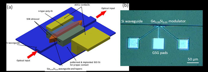
Tensile Strained Ge0.99 Si0.01 EA Modulator Arrays for Integrated Broadband Modulation
Danhao Ma1, Yiding Lin2, Ruitao Wen3, Lionel Kimerling1, Jurgen Michel1
1 Department of Materials Science and Engineering, Massachusetts Institute of Technology, USA
2 School of Electrical and Electronic Engineering, Nanyang Technological University, Singapore, Singapore 3Department of Materials Science and Engineering, Southern University of Science and Technology, China
e-mail: madanhao@mit.edu
ABSTRACT
Electronic and photonic integrated circuits serve as a promising platform for telecommunications and sensing applications. A one-for-all tensile strained Ge0.99 Si0.01 modulator array design is proposed to cover a broad telecommunication band with multiple modulators designed and fabricated simultaneously in a single lithography and patterning flow. Modulators with the width from 0.5μm to 3μm demonstrated the absorption edge shift from 1533nm to 1566nm, relating to an array wavelength operation from 1526nm to 1575 nm, with an extinction ratio of 4.5dB at 3V reverse bias. This strain engineering innovation can be applied not only to Ge and GeSi materials, but also to III-V materials for light-emitting, photodetecting, wavelength filtering, and sensing applications. This approach allows electronic – photonic integrated systems to be developed with a simpler device layout, higher device yield, and lower fabrication cost.
Keywords: strain, germanium, waveguide device, modulator, integrated photonics, low-cost fabrication