
Statistical analysis of passive components manufactured in a thick silicon nitride platform (Student Paper)
Juan Fernández1,2, Joan Felip1, Jose Serrano1, Raffaele Caroselli1, Bernardo Gargallo1, David Domenech1, Pascual Muñoz1,2
1 VLC Photonics S.L., c/ Camino de Vera s/n – 46022, Valencia – Spain
2 Universitat Politènica de València, c/ Camino de Vera s/n – 46022, Valencia – Spain
e-mail: juan.fernandez@vlcphotonics.com
ABSTRACT
In this paper, the statistical analysis of the measurements of passive components manufactured in a thick silicon nitride platform is presented. The devices studied are Asymmetric Mach-Zehnder interferometers (AMZI) and 1×2 and 2×2 Multimode Interference Couplers (MMI). Components from four different Multi-Project-Wafer runs [1], have been designed, manufactured and tested. Each run yielded two wafers and two dies per wafer have been measured and reported. The Asymmetric Mach-Zehnder interferometers were used to evaluate the propagation parameters of the strip waveguides employed in the designs. These parameters are: the propagation losses, the modal effective index and the group index. The multimode interference couplers (MMI) have been employed to evaluate the fabrication tolerances. By collecting and evaluating this statistical data across multiple dies, wafers and runs we have concluded that the designs evaluated are robust and the manufacturing process is stable within the tolerances provided by the foundry. This is fundamental for high-volume, high-yield commercial applications for future market developments in thick silicon nitride platforms as quantum, comb generations, LIDAR systems, etc.
Keywords: thick silicon nitride, silicon nitride, yield, manufacturing.
Polarization insensitive tunable hitless filter for extended C band (Student Paper)
Maziyar Milanizadeh, Matteo Petrini, Francesco Morichetti and Andrea Melloni
Dipartimento di Elettronica, Informazione e Bioingegneria – Politecnico di Milano,
Milano, 20133 Italy
e-mail: andrea.melloni@polimi.it
ABSTRACT
Controllable loss induced through variable optical attenuators integrated in microring resonators is exploited to implement a novel hitless tuning scheme for silicon photonic WDM filters. The proposed concept is demonstrated in a polarization insensitive architecture operating across the extended C-band.
Keywords: Photonic Integrated Circuits, Silicon Photonics, Ring Resonators, Optical Add Drop, Hitless Filters.
Building large scale photonic integrated circuits in suspended gallium arsenide: Passives
Pisu Jiang 1 and Krishna C. Balram 1
1 QET Labs, University of Bristol, Woodland Road, Bristol BS8 1UB, UK
e-mail: krishna.coimbatorebalram@bristol.ac.uk
ABSTRACT
The spectacular success of silicon-based photonic integrated circuits (PICs) in the past decade naturally begs the question of whether similar fabrication procedures can be applied to other material platforms with more desirable optical properties. In this work [1], we demonstrate the individual passive components (grating couplers, waveguides, multi-mode interferometers and ring resonators) necessary for building large scale integrated circuits in suspended gallium arsenide (GaAs). Implementing PICs in suspended GaAs is a viable route towards achieving optimal system performance in areas with stringent device constraints like energy efficient transceivers for exascale systems, integrated electro-optic comb lasers, integrated quantum photonics, cryogenic photonics and electromechanical guided wave acousto-optics.
Keywords: Photonic integrated circuits, grating couplers, rib waveguides, ring resonators, waveguide couplers,multimode interferometers
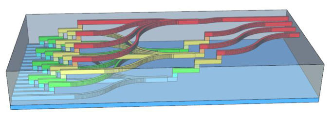
3D Photonic Integration: Cascaded 1×1 3D Multi-mode Interference Couplers for Vertical Multi-layer Connections
Madeleine Weigel1, Moritz Kleinert1, Hauke Conradi1, Anja Scheu1, Martin Kresse1, Crispin Zawadzki1, David de Felipe1, Norbert Keil1, Martin Schell1
1 Fraunhofer Heinrich Hertz Insitute, Einsteinufer 37, 10587 Berlin, Germany
e-mail: madeleine.weigel@hhi.fraunhofer.de
ABSTRACT
A vertical interconnection across four stacked polymer waveguide layers using 3D multi-mode interference couplers (3D MMIs) is presented. This system bridges a vertical distance of 21.6 μm with a minimum on-chip loss of 2.5 dB. The multi-layer connection is a basic element for novel applications, like large-scale optical switching matrices with a waveguide crossing-free architecture and a small footprint.
Keywords: 3D photonic integration, polymer waveguide, multi-layer waveguide system, vertical multi-mode interference coupler.
Silicon Nitride Waveguides and Spot Size Converters with < 1.76 dB Loss Over Broad Wavelength Range from 1010 nm to 1110 nm for OCT Applications
Piotr. J Cegielski1, Stephan Suckow1, Anna Lena Giesecke1, Caroline Porschatis1, Holger Lerch1,
Maik Lütticke1, Bartos Chmielak1, Max C. Lemme1,2
1AMO GmbH, Otto-Blumenthal-Str. 25 52074 Aachen,
2Chair of Electronic Devices RWTH-Aachen University, Otto-Blumenthal-Str. 25 52074 Aachen,
e-mail: cegielski@amo.de
ABSTRACT
In this work the first spot size converters for edge coupling into the silicon nitride waveguide platform with coupling loss lower than 1.76 dB in the wavelength range from 1010 nm to 1110 nm are presented. The spot size converters consist of a SU-8 waveguide matching the mode field diameter of a single mode fiber. High quality end facets of SU-8 are prepared by carefully dicing through the SU-8 waveguides without edge polishing. The SU-8 waveguide mode is converted to the Si3N4 waveguide mode by an inverse taper. The Si3N4 taper tips are narrower than 200 nm, which is required to avoid reflections. They are fabricated using cost efficient i-line projection lithography with a nominal resolution of 500 nm. The Si3N4 waveguide propagation losses are as low as 0.4 dB/cm.
Such low loss broadband photonic platform can find use in e.g. retinal optical coherence tomography. The measured coupling loss is comparable to the best available devices for longer wavelengths.
Keywords: silicon nitride, integrated photonics, spot size converters, edge coupling
More information about Photonics Applications.